Thin-Film Material Science and Processing
Thin films are important because they offer the potential for low-cost processing with minimal material usage while fulfilling application requirements. Importantly, this can enable cost-effective applications for expensive raw source materials. Thin films also can enable applications where low weight and mechanical flexibility are crucial.
Capabilities
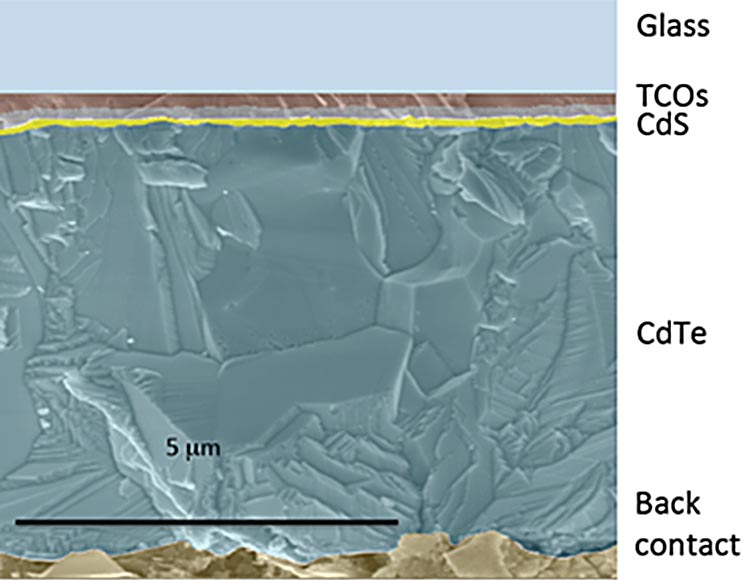
Cadmium Telluride PV
Our capabilities and expertise in cadmium telluride (CdTe) PV consist of polycrystalline films deposition and device processing including buffer layers, transparent conducting oxides and contact materials, epitaxial film growth and device processing, CdTe doping expertise, and deposition onto flexible substrates.
Contact
Matt Reese
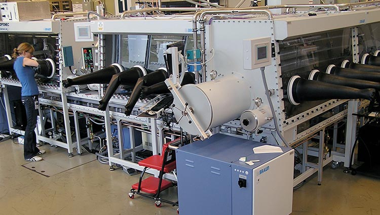
Copper Indium Gallium Selenide PV
Our capabilities and expertise in copper indium gallium selenide (CIGS) PV consist of polycrystalline films deposition and device processing including buffer layers, transparent conducting oxides and contact materials, deposition onto flexible lightweight substrates, and large-area (6"x6") deposition.
Contact
Lorelle Mansfield
Lorelle.Mansfield@nrel.gov
303-384-7884
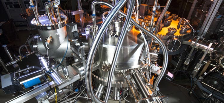
Atmospheric Processing Platform Capabilities
At the Process Development and Integration Laboratory, the Atmospheric Processing Platform (APP) offers powerful capabilities with integrated tools to deposit, process, and characterize PV materials and devices. Different methods are used to deposit ("write") materials onto a variety of substrates, which are then further processed using rapid thermal processing. What is unique about the APP is that these processes are performed at atmospheric pressure, without the requirement for expensive vacuum equipment.
Contact:
Rosemary Bramante
Vapor Barrier Diffusion Measurements
Barriers to oxygen and moisture are critical packaging components for a wide variety of industries. The requirements of each application vary significantly, with differing needs for cost and permeation rates. We have developed a quantitative high-throughput technique that can measure many barriers in parallel with unsurpassed sensitivity.
Contact:
Matthew Reese
Material Characterization with X-Rays
Our X-ray capabilities include X-ray diffraction (XRD) and X-ray fluorescence (XRF) characterization. Associated capabilities are a hot stage for XRD, mapping capabilities for XRD and XRF, and micro-XRF mapping.
Contact
Philip Parilla
Philip.Parilla@nrel.gov
303-384-6506
Contact
The Materials Science Center is part of the Materials, Chemical, and Computational Science directorate, led by Associate Lab Director Bill Tumas.
Share
